Advanced packaging solutions for photonics, RF and microelectronics

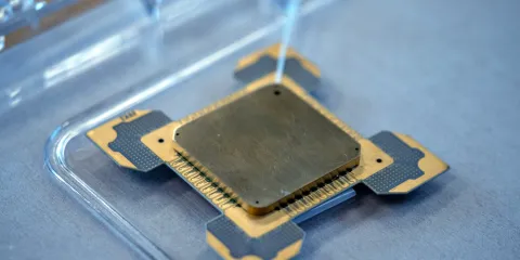
Advanced packaging solutions of RF and photonics components for applications in 5G and 6G, aerospace and defence and security is needed to achieve low power loss, efficient signal isolation and reliable functionality. Use of low-temperature cofired ceramics (LTCC) packaging substrates is one of the best options for this thanks to its superior electrical properties. With LTCC packaging it is possible to create miniaturised communications and sensor modules operating at very high frequencies, as well as photonics modules with low loss optical interfaces, high speed electronics and better thermal management.
Key facts about advanced packaging solutions for Photonics, RF and microelectronics
We develop and supply packaging prototypes that can readily be transferred to industrial volume production.
LTCC carriers, circuits and modules with optical, electrical and RF functionality are a core part of our advanced packaging offering.
Our solutions benefit different industries, incl. telecom & wireless, automotive, sensor & opto-packaging, medical, and military & space

At VTT, we specialize in developing and manufacturing of hybrid integration technologies for advanced photonics and mm-wave modules, enabling path from chips to functional components, modules and systems. We combine our novel approaches with mature fabrication processes to create solutions that respond to each customer’s specific needs.
We have a long track record in advancing assembly and module packaging for various industries and applications, and we take pride in making sure that your device operates even in the toughest environments.
Our world-class research infrastructure gives us versatile capability to do prototyping, piloting, and small volume manufacturing. We have quick and flexible development cycles, and we are able to do customer specific fabrication runs. This allows our customers to rapidly evaluate the feasibility of their micromodule concepts.
Special benefits to our customers:
Combination of state-of-the-art and novel fabrication approaches with already mature processes
Access to VTT’s very extensive partner network on research, photonics component suppliers, high-volume production, system integration, etc.
Tailored LTCC solutions from design to manufacturing
VTT is a leading expert in Multilayer Ceramics (LTCC) solutions for industries. We offer our customers R&D, prototyping and contract manufacturing of LTCC carriers and modules with optical, electrical and RF functions.
Our capabilities cover a range of solutions and services to meet the individual needs of each customer and project:
- We offer prototyping, piloting, small volume manufacturing of LTCC substrates
- Quick and flexible development cycles
- Customer specific fabrication runs
- Our LTCC solutions enable
- Multi-technological system-on-package integration based on LTCC substrates
- RF components up to mm-wave frequencies
- Miniature packaging of MEMS and photonics devices, e.g. sensors and fiber-optic modules
- We develop solutions are also suited for extreme environments, including military, aeronautics and space
Photonics and RF Micromodules
VTT has over 30 years of experience on advanced photonics hybrid-integration and packaging technologies. High-performance photonics modules and instruments are implemented using in-house manufacturing and assembly processes and multi-disciplinary design and testing capabilities. We advise and support our customers and partners toward the most suitable technology choices and work together to design and develop tailored solutions.

- Assembly and packaging at wafer, chip, and module level
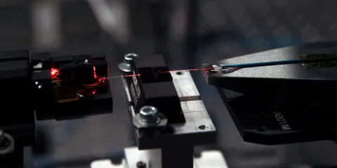
- High-precision photonics assembly
- Fiber pigtailing, also with fiber arrays
- Flip-chip, die attach, soldering and adhesive bonding
- Encapsulation and packaging for reliability, including hermetic sealing
- Thermal management with advanced solutions
- High-performance electronics integration up to mm-wave frequencies
- System-on-Package
- Photonics integrated circuit (PIC) packaging
- Design for integration, manufacturing and reliability, including thermal design
We have worked on solutions and applications for various industries, including sensing, communication, space, military, and consumer devices.
Dedicated cleanroom facilities for advanced integration and packaging
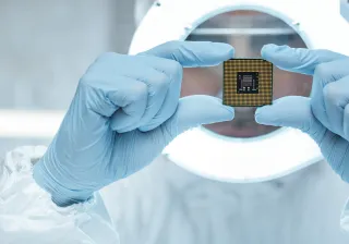
VTT’s Micromodule Centre in Oulu is a cleanroom facility dedicated to advanced integration and packaging activities for photonics and electronics components and systems. It consists of versatile design tools and fabrication and testing equipment applied by experienced researchers and technicians. Our cleanroom facilities allow our customers to flexibly evaluate and demonstrate the feasibility of their device concepts, optimize designs and manufacturing processes, and launch production.
In our facilities we conduct processes related to hybrid integration, assembly and packaging. Our expertise includes multilayer ceramics, thin film, bonding, soldering, fiber pigtailing, high-precision assembly, encapsulation, hermetic and vacuum sealing, etc.
MicroModule Centre
- 600 m² effective clean room area
- Classes 100 (ISO 5) – 10000 (ISO 7)
- Hybrid integration, assembly and packaging
- LTCC and thick film ceramics
- Lithography and nanoimprinting
- Extensive characterisation and testing equipment

From concept to product – how to work with us on advanced packaging and LTCC?
Get in touch with us to kick-start the development of your customized packaging solution! Our services include
-
Research and development
-
Confidential contract research
-
Packaging prototyping
-
Small to medium volume manufacturing
Project highlights
PREIN
VTT is part of PREIN – The Flagship on Photonics Research and Innovation. PREIN is a Photonics Research and Innovation platform focusing on light-based solutions from scientific excellence to industrial and societal impact. Together with our partners at PREIN, we develop photonics and light-based technologies that play a central role in all areas of modern life, including in telecommunications, biomedicine, health care, energy and environment, manufacturing, and consumer products.
ACTPHAST and PhotonHub Europe
Both ACTPHAST and PhotonHub Europe initiatives provide one-stop-shop access to a wide range of existing cutting-edge photonics technology platforms from Europe’s top research centres. The photonics expert services of can be subsidized to European companies and researchers using existing EC grants.
VTT’s photonics integration and packaging expertise is offered also through ACTPHAST and PhotonHub.
MACQSIMAL
macQsimal is an EU-funded research project which designs, develops, miniaturizes and integrates advanced quantum-enabled sensors. VTT has developed ceramics-based packaging solutions for atomic clocks, gyroscopes, and optically pumped magnetometers.
https://www.macqsimal.eu/
Meet some of our experts

Expert on integration and packaging technologies with extensive experience on photonics devices and modules.

Expert in ceramics manufacturing and RF/microelectronics packaging.
Contact us here!
Featured service: Photonics
Do you want to know what more we do in the area of photonics? VTT's photonics research solves global and industrial challenges ranging from affordable healthcare and climate change to consumer electronics and autonomous vehicles.

