Medical microelectronics

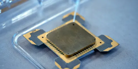
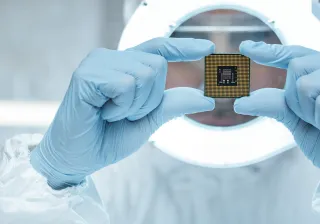
Microelectronics is an essential field for medical technology. These miniaturised and energy efficient devices can be tailored for application-specific needs. By leveraging our world-class expertise and cutting-edge infrastructure, we innovate new sensors for challenging environments, seamlessly integrating them into modules and systems.
Key facts
Medical microelectronics are energy-efficient, application-specific devices.
VTT has decades of experience in developing medical microelectronics and the ability to innovate new sensors for e.g. diagnostic testing of blood, body fluids and tissue or for measuring gas or liquid flow.
Our multi-disciplinary expertise and in-house R&D infrastructure allow us to support you throughout the entire development cycle, from research to piloting and small-scale fabrication.

The world is increasingly hungry for more accurate health data. With better data, healthcare providers can significantly improve the quality, efficiency and effectiveness of care by making informed decisions and tailoring treatments to individual needs.
Medical microelectronics enables the seamless integration of sensors, actuators, cameras and microprocessors within medical devices, thus driving the implementation of data-driven healthcare practices. Small in size, these devices can be used for specialised measurements and sensing applications and fitted, for example, even inside the human body. Medical microelectronics open up new possibilities in identifying conditions earlier, diagnosing diseases as well as guiding treatment and rehabilitation.

Why VTT?
At VTT, we provide expertise in advanced sensor design combined with in-depth knowledge of cutting-edge health applications. We can also seamlessly integrate the sensors and components we design, for example, into patches, medical aids, wearables and even into implantable devices.
We are particularly adept at designing microelectronics for demanding environments. As the operating environments change, so must the design and configuration of the device. All the microelectronics we design are application-specific, tailored to your needs.
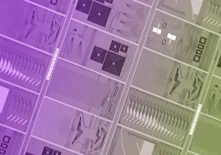
Our extensive in-house R&D infrastructure guarantees we can support you throughout the entire development cycle, from research to piloting and small-scale implementation. Our unique infrastructure covers everything from the manufacturing of nano- and microelectronics to integrated photonics and printed electronics.
To ensure the viability of the solution, we can turn the ready components into proofs of concept or demonstrators. Thanks to our strong analytics capabilities, we can also perform the data processing.
We also offer our large IP portfolio for licensing.
Our medical microelectronics offering
MEMS applications
A specific spearhead in VTT’s MEMS expertise portfolio are thin film (Sc)AlN-based, highly miniaturised, low power, lead-free piezoelectric ultrasonic transducers (PMUTs). These ultrasonic sensors can be applied to gas and liquid flow measurements, structural tissue analysis, imaging and vital sign sensing. The PiezoMEMS technology lends itself also to biosensing for analyte and virus detection.
Our surface-MEMS-based absolute and differential pressure sensors and sensor matrices can be tailored and used in the most extraordinary applications imaginable, including catheters and implants.
We also integrate MEMS devices into operational micromodules and smart edge sensor systems. When applicable, we design an application-specific integrated circuit (ASIC) or an analogue front-end to read and interpret the MEMS sensor data. A customised readout part guarantees the smallest possible size and best form factor for the application, as well as low power consumption and low noise.
Hyperspectral imaging applications
Going beyond the Red-Green-Blue (RGB) colour space and spectral limitations of the human eye unlocks countless opportunities, such as detecting biological processes and conditions in humans. Hyperspectral technologies provide a way to analyse skin changes and detect skin cancer, for example.
The hyperspectral technologies we have developed enable mobile, low cost and high-performance visible and short-wave infrared hyperspectral imaging. Our tailored hyperspectral cameras with advanced image sensors and optics design can be used in any application and at any wavelength from ultraviolet to long-wave infrared.
2D materials applications
Graphene and other 2D materials provide new functionalities in electronics, photonics and sensing applications. We have actively participated in graphene related research projects for over a decade and are also one of the 2D experimental pilot line sites. We provide graphene R&D services for sensing, photonics and electronics with in-house processing with high yield on 200 mm wafers.
Graphene biosensors can be used in various applications. The most typical graphene-based biosensors rely either on field effect or surface plasmon polariton based sensing. Field-effect-based biosensing offers interesting opportunities with its label-free sensing capabilities, enabling the development of significantly more cost-effective sensors compared to conventional optical sensing methods.
We have developed a post-CMOS integrated graphene biosensor platform that enables the characterisation of large sensor arrays with multi-analyte sensing. Our standard biosensor structure and process can be modified and developed to meet the requirements of various custom biosensors. By adding a custom ASIC readout as well as readout electronics, the biosensor can be integrated to a portable system. We also offer services related to biofunctionalisation and bioanalysis with graphene-coated SPR and QCM chips.
Integrated photonics applications
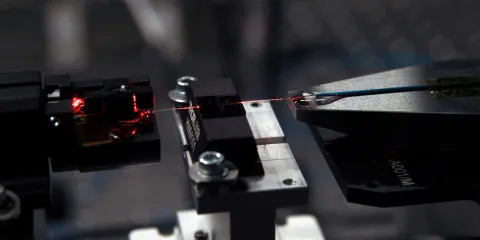
Integrated photonics solutions combine optical components and functions onto a single chip, enabling a small footprint, high performance and low loss. In the field of medical technology, they enable advancements in diagnostics, laser-based imaging and monitoring, among other things.
We have an extensive heritage in developing integrated photonics solutions, dating back to the 90s. Our photonic integrated circuits (PICs) have helped minimise, for example, the cost, power consumption and size of wearable devices.
Case: Rockley Photonics
Rockley Photonics is at the vanguard of integrated photonics. The company integrates photonic integrated circuits (PICs) with advanced microelectronic circuits (ICs) to develop miniaturised optical sensors that perform well in consumer applications. Rockley Photonics has collaborated with VTT since 2014 on R&D and the implementation of its rapid silicon photonics prototyping and commercialisation needs.
Some questions we can help you with
- Can you design a custom PMUT for us?
- Can you help us develop a process flow for our biosensor?
- How could we be more cost-effective?
- How can we make our medical microelectronics more energy-efficient?
- Can you pilot our solution?
How to work with us
Contact us!
Tell us what you want to do, and we will figure out how to do it. No project is too small or too ambitious – we would love to hear from you. After the initial assessment, we might be able to offer some of the following options:
-
Customised partnership
Every research case is unique, and we’re happy to tailor our services to your needs. We’ll take you from idea to prototype without hassle.
-
Cooperative project
We frequently participate in research and development projects with multiple business partners and funding agencies. In cooperative projects the risk is split between multiple organisations, and everyone benefits from the results.
-
Our networks and ecosystems at your disposal
We are happy to put you in touch with the ideal sparring and development partner.
Related infrastructure
Meet our team


