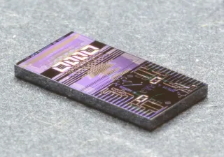
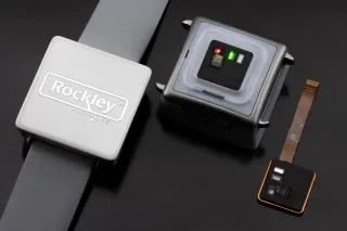
Photonic integrated circuits (PICs) minimise the cost, power consumption and size of wearable devices. In partnership with VTT, Rockley Photonics is developing pioneering sensors and taking them to mass production.
Key facts:
Versatile and affordable health & well-being wearables are now available for the consumer market
Wearable sensors could become the largest market for integrated photonics
Thick silicon waveguides enable extreme broadband sensors that are accurate, small and energy efficient
Founded by integrated photonics pioneer Andrew Rickman in 2013, Rockley Photonics is in the vanguard of integrated photonics. It builds on the heritage of two former silicon photonics companies, Bookham and Kotura. After going public in a SPAC merger with SC Health in August 2021, the company has been traded on the New York Stock Exchange (NYSE) at an initial valuation of over a billion dollars.
Silicon photonics has serious potential in consumer applications
Rockley integrates photonic integrated circuits (PICs) with advanced microelectronic circuits (ICs) to develop miniaturized optical sensors that perform well in consumer applications.
Most companies operating in the integrated photonics field develop PICs with submicron waveguide dimensions. The PICs have mainly been used in high-speed optical communication in data centres and to some extent in industrial and medical sensing and laser-based imaging (lidar).
Rockley Photonics, however, envisioned the potential for a platform based on thick silicon waveguides to broaden the applications of silicon photonics into a wider range of volume applications, in particular consumer devices. The company focused their R&D efforts on creating wearable sensors that can measure multiple biometrics simultaneously and be used in a variety of device forms.
Micrometre-scale (> 1 µm thick) silicon waveguides are a good match for consumer devices. Using thick waveguides:
- minimises optical losses
- eases dense integration of III-V laser diodes
- improves wavelength accuracy and precision for high manufacturability
- maintains small chip footprint.
Thick waveguides also allow operation over a very broad range of wavelengths. This is critical for expanding the range of biomarkers that can be monitored and for creating a platform that can be applied to a range of products in consumer wearable and medical technology markets.

First steps of the R&D collaboration
Since its beginning, Rockley Photonics has been a fabless company. Instead of spending resources on running their own manufacturing facility, Rockley has concentrated on cutting-edge research and developing the best possible custom silicon photonics platform from the ground up.
Rockley needed a fab partner but combining agile R&D with mass production is not trivial. High-volume microelectronics foundries are reluctant to offer small-volume R&D and pilot runs. Smaller facilities, such as university laboratories, typically cannot provide rapid turn-around, process repeatability, high yields and commercial manufacturing services.
Fortunately, VTT's Micronova clean room facility offered flexible R&D services and pilot production combined with 17 years of experience in the development of micrometre-scale silicon waveguide technology. In addition to R&D and pilot production, VTT offered the ability to transfer the technology to large-volume fabs.
As a result, Rockley has collaborated with VTT since 2014 on R&D and the implementation of its rapid silicon photonics prototyping and commercialisation needs.

Complementary capabilities and facilities
VTT was an ideal partner for Rockley, as VTT had
- strong expertise in micrometre-scale silicon photonics
- fabrication and test equipment to conduct the research Rockley needed to develop and refine their processes
- a process line for small-scale pilot manufacturing in the Micronova clean room facility
- a wide contact network of international research, development and commercialisation partners.
Only a few organisations in the world could offer the combination of R&D and manufacturing services for micrometre-scale silicon waveguides, and nobody had the expertise that VTT had accumulated in this field. Their capabilities have proven to be a great help to Rockley as we work to bring photonics-based sensing solutions to the mass market.
Rockley set up a base and built a team in VTT’s facilities. Together the two companies started to develop and prototype Rockley’s silicon photonics and fabrication processes, along with supporting the transition to large volume fabs. Rockley wanted the projects to move fast and proceed to a demo phase as quickly as possible.
We immediately understood the potential and requirements of the partnership and upscaled our team fast to enable rapid and flexible collaboration with Rockley.
Rapid growth into sensor mass production
With VTT’s help, Rockley developed its PIC technology platform, grew its own multi-disciplinary engineering team and developed full-stack clinic-on-the-wrist sensor solutions.
While VTT focused on fabrication and supporting continued sponsored research, development and testing of the base PIC technology process, Rockley led the design of the PICs, and co-designed electronics, packaging, and algorithms to make the sensor products.
As the core silicon photonics process was designed for mass production from the beginning, Rockley could easily use its silicon photonics platform in large foundries to upscale manufacturing. This opened the floodgates for a cost-efficient sensor platform that could easily be applied in a variety of sensor products.
This led to Rockley demonstrating their sensor technology to several of the largest consumer electronics and medical device companies, which now aim to use the technology in their wearable products. Potentially, Rockley’s new sensors could enable the non-invasive measurement of, for example, blood sugar, blood pressure, blood alcohol content and lactate.
The project has wide-ranging consequences:
- Consumers get quality wearables for health and well-being with more accurate readings and more functionality.
- Rockley now has mass-produced standard sensors that have a significantly bigger market potential than traditional PIC-based products.
- The small and power-efficient chip-sized sensors help reduce the impact of climate change by using less raw materials and reducing power consumption.
Partnership will grow with commercialisation
The partnership between VTT and Rockley Photonics has been mutually beneficial. While both are pioneers in integrated photonics and thick silicon waveguides, the collaboration has enabled the organisations to learn from each other and deepen their knowledge. While Rockley has benefited from using VTT’s R&D facilities, VTT benefitted from working with the absolute best of the industry.
"Having VTT as our early fab partner enabled us to get to market with prototypes faster than would have been possible anywhere else. Having them as a continuing R&D partner also provides world-class R&D capabilities for next generation integrated photonics, healthcare and medical technologies and solutions," says Aaron Zilkie, CTO Photonics at Rockley.
Having produced technology that improves on existing wearable solutions, VTT and Rockley’s collaboration will spread to other areas, such as developing new applications for the sensors.
"I see great potential to deepen our relationship with Rockley. VTT has vast expertise in regulations and standards and a network of contacts that are interested in state-of-the-art wearable technology. Continuing quality R&D is a priority, but we can also find synergies in commercialising existing solutions," Aalto concludes.


